

MONTSERRAT GALCERAN MESTRES
SENIOR RESEARCHER
SENIOR RESEARCHER
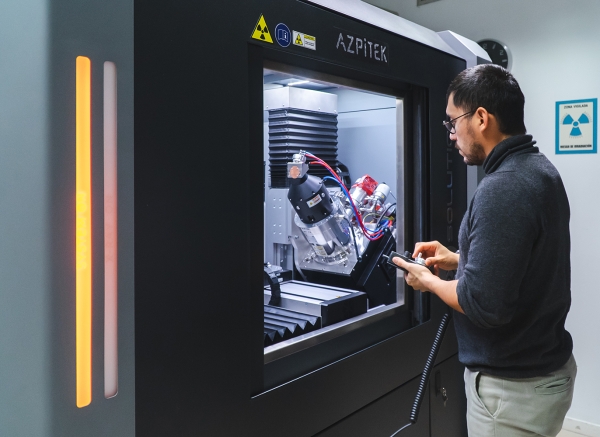
The Electron Microscopy Platform is the center for the microstructural characterization of the materials developed at CIC energiGUNE. Ultimate spatial resolution and electron diffraction analysis combined with the simultaneous acquisition of spectroscopic data are used to guide the synthesis of new materials as well as to monitor structural developments induced under electrochemical reactions ex-situ.
The platform offers electron microscopy measurements by using a Transmission Electron Microscope (TEM) and a Scanning Electron Microscope (SEM), as well as support service with relevant sample preparations techniques such as ion milling. The platform counts with a dedicated laboratory for sample preparation and especially offers equipment for mechanical cutting and polishing, coating, embedding, plasma cleaning and ion beam thinning.
The services are provided for different research groups at CIC energiGUNE and for external users like other research centers or other public organization and also to commercial and private companies.
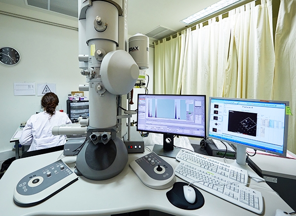
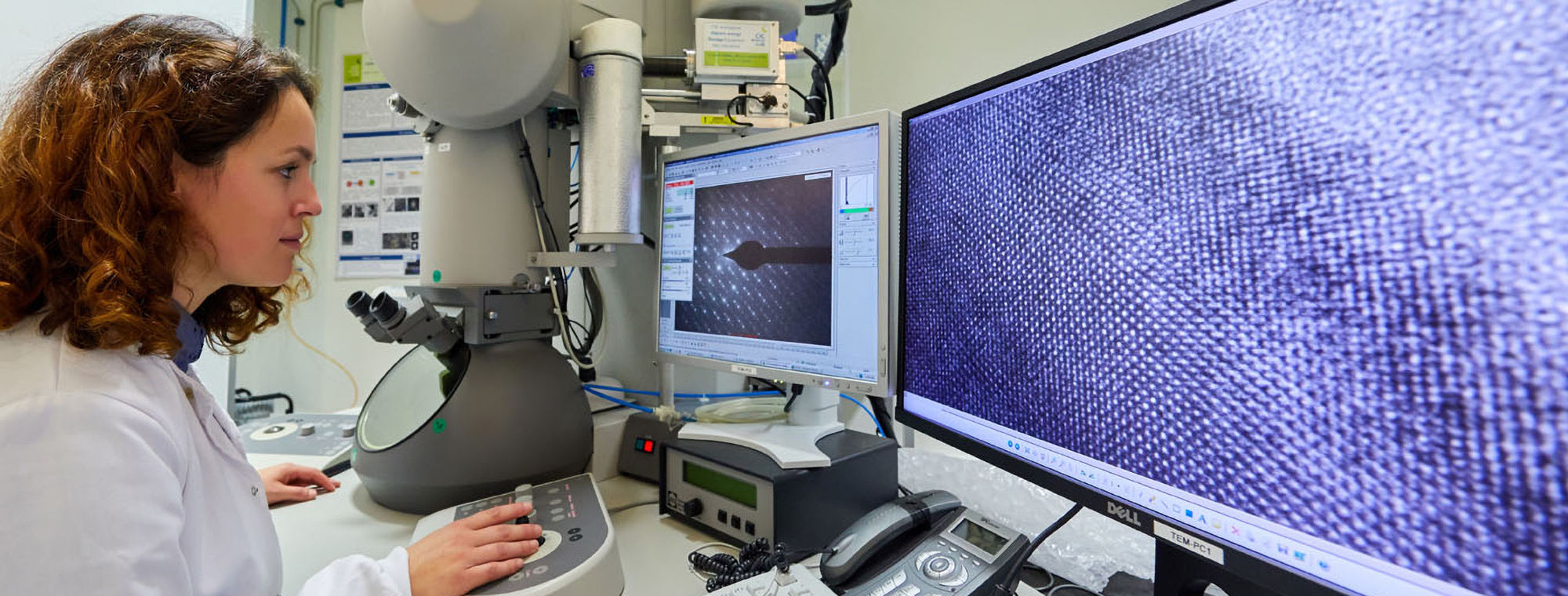
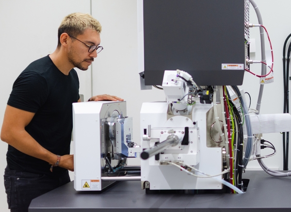
The Tecnai G2 F20 is a 200kV field emission gun (FEG) high resolution TEM/STEM enabling to solve a wide variety of materials science challenges in an easy and fast way. The FEI Tecnai G2 excels in versatility and flexibility by combining high performance in TEM/STEM imaging modes and EDX spectroscopy. A key feature of this microscope is the low energy spread of the electron beam (0.7 eV@200kV or less) which combined with the SuperTwin objective lens, with a Cs of 1.2 mm, allows the determination of the physical and chemical properties at atomic resolution.
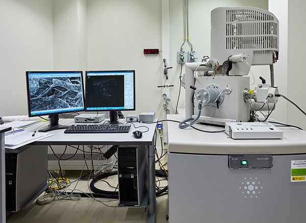
The Quanta 200 FEG is a high-resolution microscope capable of running in 3 different modes: high vacuum, variable pressure and environmental modes. The working voltages of the Quanta 200FEG vary between 3kV (low vacuum mode) and 30 kV (high vacuum mode). These features allow this microscope to handle different type of specimens even uncoated, non-conductive samples as well as wet samples that require being above the vapor pressure of water. The combination of high output thermal field emission (> 100nA beam current) with a high sensitivity (18 mm) allows get final resolution until 3-5 nm. Among the different detectors installed in the microscopes for morphological analysis of samples, the presence of the backscattered electron detector giving images with atomic contrast allows to have access to the elemental composition of the samples. One additional key of this microscope is the transfer chamber for sample sensitives to the air (from Gatan company) making possible to study Li- and Na- based materials and any type material sensitive to the moisture or the oxygen from the atmosphere.
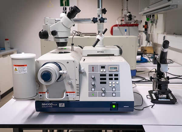
The IM4000Plus Ion Milling System utilizes a broad, low-energy Ar+ ion beam milling method to produce wider, undistorted cross-section milling or flat milling, without applying mechanical stress to the sample. This system provides two milling configurations in a single instrument for flattening and cross sectioning samples. The range of materials and samples that can be prepared by this technique goes further than hard matter. In fact, thanks to the additional modes installed on our equipment: the cryo unit and the transfer chamber for sensitive materials, high-quality sectioning can be achieved with the IM4000Plus even with "soft" samples such as paper, polymers, and powders.
If you want to know the latest trends in energy storage and new developments in research, subscribe.
If you want to join a top-level team, collaborate with specialists in multiple disciplines or tell us about your concerns, don't think twice...